This user evaluation report is provided by ”zealsoft” from ElecFans. It involves the analysis and testing of the ARM-end example
"pcie2screen" on MYIR’s MYD-JX8MMA7 development board, along with an explanation of the modifications made to the
FPGA-end program.
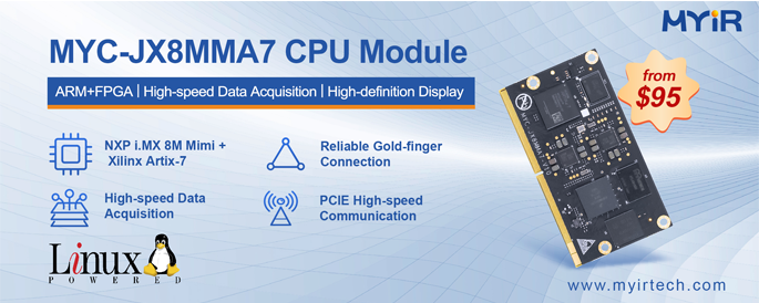
The MYD-JX8MMA7 Development Board is built around the MYC-JX8MMA7 CPU Module is an ARM+FPGA based SoM based
on NXP’s i.MX 8M Mini processor with up to 1.8GHz quad ARM Cortex-A53 and 400MHz Cortex-M4 cores. This ARM processor
provides robust data processing, control, communication and display capabilities. Additionally, the Xilinx XC7A25T Artix-7 FPGA
acts as an auxiliary processor, optimizing cost and transceiver usage while achieving high-speed data acquisition and
processing. The MYD-JX8MMA7 Development Board is an all-in-one evaluation platform suitable for a variety of applications.
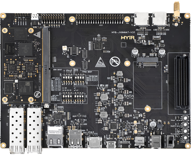
MYD-JX8MMA7 Development Board
Part 1
Testing example pcie2screen
The "pcie2screen" example is provided for the MYIR_PCIE_5T_CMOS project of the MYD-JX8MMA7 development board. Its purpose is to display the video captured by a camera connected to the FPGA. After running this program, a window with the title "demo" will appear on the screen.
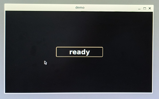
Press the "ready" button, the demo window will display a continuous video, indicating that the camera, DDR and PCIe interfaces are all functioning properly. If the camera is not connected, the program will display disordered images.
The source code for this test example is not included in the SDK and can be requested from MYIR. The example is developed using Qt and OpenGL technology. The program is mainly classified as below:
MainWindow: QMainWindow subclass for displaying windows
uOpenglYuv: QOpenGLWidget subclass for displaying captured images.
The initializeGL function of this class is used to initialize OpenGL. The paintGL function is used for drawing images, the core statement of which is:
glTexImage2D(GL_TEXTURE_2D, 0, GL_RGBA, vW, vH, 0, GL_RGBA, GL_UNSIGNED_BYTE, pRGB);
The "pRGB" stores data that is read from the FPGA. From this sentence, we can find the image format required by the program.
* xdma_ getImg: mainline class
* xdma_ program: encapsulates the RIFFA interface, the read_ pack is used to read FPGA data and is called by the main thread in a loop. Its functions are defined as follows:
int xdma_programe::read_pack(char *pData, int len)
{
//int buffer[1920 * 1080];
//int buffer[1024 * 768];
int buffer[1280 * 720];
int i;
if(dev_fd != NULL)
{
fpga_send(dev_fd, 0, buffer, len / 4, 0, 1, 25000);
fpga_recv(dev_fd, 0, buffer, len / 4, 25000);
memcpy(pData, (char *)buffer, len);
return len;
}
else
{
return 0;
}
}
It can be seen from the function that before reading data each time, the function will write data to FPGA at first (Data is meaningless and it is related to the state of the FPGA), and reads an entire frame of data each time.
Part2
Modification of FPGA terminal program
The logic control of FPGA end is in chnl_tester.v, it defines a state machine to control data receiving and sending. The state machine is defined as follows:
always @(posedge CLK or posedge RST) begin
if (RST) begin
rLen <= #1 0;
rCount <= #1 0;
rState <= #1 0;
rData <= #1 0;
vout_vs_r <= #1 0;
end
else begin
case (rState)
3'd0: begin // Wait for start of RX, save length
if (CHNL_RX) begin
rLen <= #1 CHNL_RX_LEN;
rCount <= #1 0;
rState <= #1 3'd1;
end
end
3'd1: begin // Wait for last data in RX, save value
if (CHNL_RX_DATA_VALID) begin
rData <= #1 CHNL_RX_DATA;
rCount <= #1 rCount + (C_PCI_DATA_WIDTH/32);
end
if (rCount >= rLen)begin
rState <= #1 3'd2;
end
end
3'd2: begin // Prepare for TX
if (read_valid) begin
rCount <= #1 0;
rState <= #1 3'd3;
end
end
3'd3: begin // Start TX with save length and data value
if (CHNL_TX_DATA_REN) begin
//rData <= #1 data_in;
rCount <= #1 rCount + (C_PCI_DATA_WIDTH/32);
if (rCount >= rLen)
rState <= #1 3'd4;
end
end
3'd4: begin
if (vout_vs_r)
rState <= #1 3'd5;
else begin
vout_vs_r <= #1 1;
rState <= #1 3'd4;
rCount <= #1 0;
end
end
3'd5: begin
if (vs_flag) begin
rState <= #1 3'd0;
vout_vs_r <= #1 0;
end
else
rState <= #1 3'd5;
end
endcase
end
end
I don't have a camera on hand for testing, so I simply modify the program to send a blue gradient band signal.
The core changes are as follows:
……
reg [31:0] rColor = 0;
……
assign CHNL_TX_DATA = (read_en)? {rColor, rColor}:64'd0;
……
3'd3: begin // Start TX with save length and data value
if (CHNL_TX_DATA_REN) begin
//rData <= #1 data_in;
// if (rCount % 5 == 4)
rColor <= #1 rColor + 1;
if(rColor >= 255)
rColor <= #1 0;
rCount <= #1 rCount + (C_PCI_DATA_WIDTH/32);
if (rCount >= rLen)
rState <= #1 3'd4;
end
end
……
Part 03
Test result
I did not modify the test program on the ARM end and still used the pcie2screen provided by the manufacturer, just re-programmed the FPGA. See the following video for how the program works.
|

