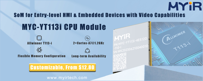
Shenzhen, China – October 16, 2023 –MYIR has launched MYC-YT113i CPU Module, offering larger capacities of external DDR3 memory options (512MB/1GB) to meet more customers’ needs while the popular MYC-YT113X CPU Module is fixed at 128MB on-chip DDR3 memory. Measuring only 39mm by 37mm, the MYC-YT113i CPU is based on Allwinner’s T113-i dual-core ARM Cortex-A7 processor and integrates 4GB or 8GB eMMC. Extended IO signals are carried out through 140-pin stamp-hole interface and 50-pin LGA pads. It is ready to run Linux and suitable for applications such as HMI, industrial automation, display and control terminals.
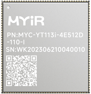 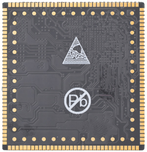
MYC-YT113i CPU Module Top-view and Bottom-view (delivered with shielding covered installed by default)
Features of MYC-YT113i CPU Module
- Dimensions: 39mm x 37mm
- PCB Layers: 8-layer design
- Power supply: 5V/1A
- Working temperature: -40~85 Celsius (industrial grade)
- Linux OS
- Allwinner T113-i processor
* Up to 1.2GHz Dual-core Arm Cortex-A7
* Single-core HiFi4 DSP
* Supports H.265/H.264 4K video decoding
- 512MB/1GB DDR3
- 4GB/8GB eMMC
- 32KB EEPROM
- 1.0mm pitch 140-pin stamp hole expansion interface + 50-pin LGA
* 1 x RGMII/RMII
* 2 x USB2.0
* 6 x UART
* 2 x CAN
* 4 x TWI
* 2 x SPI
* 1 x GPADC and 4 x TPADC
* 1 x MIPI DSI
* 2 x LVDS
* 1 x RGB
* 1 x CVBS Out (TV Out)
* 1 x Parallel CSI
* 2 x CVBS In (TV In)
* 2 x I2S
* Up to 81 GPIOs
Note: the peripheral signals brought out to the expansion interface are listed in maximum number. Some signals are reused. Please refer to the processor datasheet and CPU Module pin-out description file.
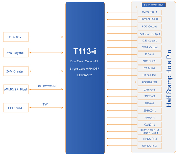
MYC-YT113i CPU Module Function Block Diagram
The MYD-YT113i Development Board is built around the MYC-YT113i CPU Module and provides a complete development platform for prototyping and evaluating purpose. Its base board has explored a rich set of peripherals and interfaces including serial ports, one Gigabit Ethernet, two USB 2.0 HOST and one USB 2.0 OTG, one Micro SD card slot, one M.2 Socket for USB based 4G/5G LTE Module with two SIM card holders, one USB2.0 based WiFi module, one GPIO/I2C/UART/SPI/CAN extension header, Audio input/output and LVDS display interface. MYIR also offers MY-WIREDCOM RPI Module (RS232/RS485/CAN) and MY-LVDS070C LCD Module as options for the MYD-YT113i Development Board to enhance the functionality of the board.
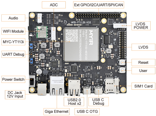
MYD-YT113i Development Board Top-view
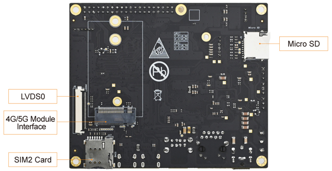
MYD-YT113i Development Board Bottom-view
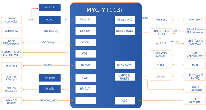
MYD-YT113i Development Board Function Block Diagram
The MYC-YT113i CPU Module is provided with three standard configurations:
MYC-YT113i-4E512D-110-I (with 512MB DDR3 and 4GB eMMC),
MYC-YT113i-8E512D-110-I (with 512MB DDR3 and 8GB eMMC),
MYC-YT113i-8E1D-110-I (with 1GB DDR3 and 8GB eMMC).
The RAM/Flash can also be customized and discount is to be offered for volume quantities which can start from only $12.80. Please inquire MYIR to get more details.
MYIR also provides OEM/ODM services to help customers accelerate their time to market and save cost.
More information about above new products can be found at:
https://www.myirtech.com/list.asp?id=741
|

